FANDA

OUR PRODUCTS

GD-Profiler 2™

Discover a Whole New World of Information with Glow Discharge Optical Emission Spectrometer

The GD-Profiler 2™ provides fast, simultaneous analysis of all elements of interest including the gases nitrogen, oxygen, hydrogen and chlorine. It is an ideal tool for thin and thick films characterization and process studies.

Equipped with an RF source that can operate in pulsed mode for fragile samples, the range of applications of the GD-Profiler 2™ goes from corrosion studies to PVD coating process control, from thin film PV development to LED Quality Control and it is used in Universities as well as in Industrial Research laboratories.

SegmentScientific
DivisionGDOES
Manufacturing Company: HORIBA France SAS

  • RF-Only generator is Class E standard and optimized for stability and crater shape allowing for real surface analysis.
  • Source can be pulsed with synchronized acquisition for optimum results on fragile samples. The use of an RF source allows analysis of conventional and non conventional layers and materials.
  • Simultaneous optic provides full spectral coverage from 110 to 800nm, including deep UV access to analyze H, O, C, N and Cl.
  • HORIBA original, ion-etched holographic gratings assure the highest light throughput and resolution for maximum light efficiency and sensitivity.
  • Patented HDD detection provides speed and sensitivity in detection without compromise.
  • On line measurement of crater depth and erosion rate with patented built in Interferometer. DIP.
  • Easily accessible sample compartment allows plenty of room for sample loading.
  • Powerful QUANTUM™ software with Tabler report writing tool.
  • CenterLite laser pointer (patent pending) for precise sample loading.

Monochromator option available only from HORIBA provides the perfect tool to increase instrument flexibility while adding “n+1” capability.

Combination of a powerful Glow Discharge source with Ultra-Fast High Resolution simultaneous optics for fast Elemental Depth Profile Analysis of conductive, non-conductive and hybrid materials.

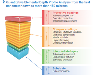
For thin & thick films – from nanometre to hundreds of microns with nanometer depth resolution.

Typical domains of applications include PV, metallurgy, LED manufacturing, corrosion studies, organic and micro-electronics, materials research & development, deposition processes optimisation, PVD, CVD, plasma coatings, automotive, Li batteries,  etc

No UHV  required.

Measurement of all elements of interest (including H, D, O, Li, Na, C, N etc) with patented High Dynamic Detectors.

Optional monochromator with Image mode and high Dynamic detection for full spectrum record and total flexibility.

Pulsed RF Source for operation in RF and pulsed RF modes with auto-matching

Differential double pumping of the source for patented SEM sample preparation

Plasma Cleaning function built in

Patented UFS for Ultra-Fast Sputtering of polymeric and organic materials

Patented DIP – built in interferometer for direct on line depth measurement

Various anode diameters and accessories for odd shape samples

Windows 10 software – Multiple copies provided for remote installations

Similar Products

Get a call back


    This will close in 0 seconds

    Request A Quote


      This will close in 0 seconds